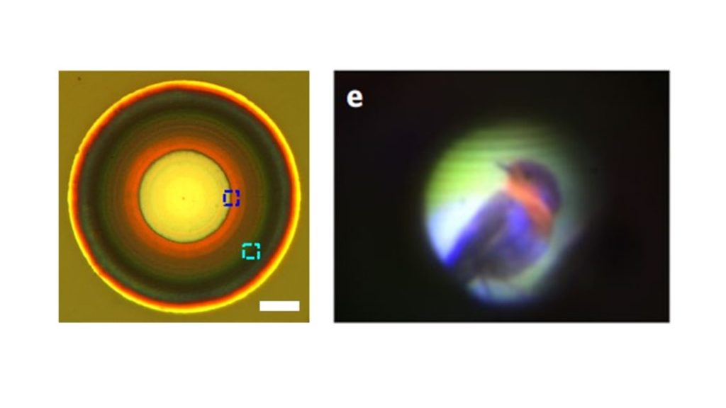
Recently, “metasurface” has become an emerging solution to address visions of “nano lens.” By arranging periodic sub-wavelength structure, metasurfaces are able to converge the incident light and even twist the light into different shapes. However, chromatic aberration, one of the most important optical problem, hasn’t been demonstrated with metasurface techniques. To address this obstacle, in 2018, Prof. Kuan (BEBI) and Prof. Tsai (Academia Sinica) successfully demonstrated a broadband achromatic metalenses by “incorporating an integrated-resonant unit element (IRUE) with the Pancharatnam–Berry phase (PBP) method”. This work had been published on Nature Nanotechnology[1].Lens have been used in various applications, such as smartphone, microscope, biological detecting device. However, traditional lens is limited by the refractive index of the material. Therefore, the thickness of lens can not shrink down to match requirements of applications. To achieve a tiny, thin, light, and precise optical device, metalens is one of the most promising solution. Metalens are capable of tailoring light properties at subwavelength resolution, such as phase, amplitude and polarization. Moreover, metalens has significant advantages of semiconductor foundry compatibility, which would benefit the development of flat optical systems in real life. To demonstrate this potential, e-beam lithography was employed by Prof. Kuan’s group to fabricate nanostructures for metalens researches. Based on the collaboration with Prof. Tsai of Academia Sinica, a broadband achromatic metalenses can be demonstrated. The developed metalens can work in the range from 400 nm to 660 nm, which coverage the visible light spectrum. As a consequence, this is the first time to show a full-color image with metalens technologies. Because of compatibility with semiconductor fabrications, the developed metalens technologies can harness momentums of semiconductor industries for different nanophotonics and integrated optics in various applications.Reference:[1] S. Wang et al., “A broadband achromatic metalens in the visible,” Nature Nanotechnology, vol. 13, no. 3, pp. 227-232, 2018/03/01 2018, doi: 10.1038/s41565-017-0052-4.
研究主題:超穎透鏡撰寫:學生 陳冠彬近年來為了解決傳統透鏡尺寸微小化的問題,超穎介面(Metasurfaces)的概念儼然成為解決小尺寸奈米光學的最佳解。超穎介面係由表面週期排列的次波長結構(Subwavelength structure)來調變入射的電磁波,進而達到不同的效果。而利用超穎透鏡來解決色散的問題一直以來都被熱烈地研究中,對此,本所管傑雄老師與中研院的團隊合作發展了革命性的新觀念-「集成共振單元」配合Pancharatnam–Berry的相位組合方式成功製作出寬頻且消色差的超穎透鏡,將超穎透鏡未來在取代傳統式透鏡的里程上推進了一大步,本篇論文已在2018年時發表在《自然奈米技術》(Nature nanotechnology)[1]。透鏡在生活中是非常廣為運用的光學元件,例如智慧型手機、醫學檢測器材、顯微鏡等等,但是礙於材料折射率的限制,目前普遍的透鏡尺寸都很大,要真正做到輕、薄、微小並且精準的元件必須仰賴超穎介面的技術。「超穎透鏡」在控制電磁波的各種特性上都有著卓越的表現,如相位、震幅和偏振等等,並且因為是透過半導體奈米技術的製程所以不但能夠製作出平面的結構並且能夠降低製造的成本,管老師團隊的電子束微影系統在製作超穎透鏡上提供了關鍵性的技術支持。儘管超穎透鏡的好處非常多,但是在解決色散的問題上依然是很大的挑戰,本次透過中研院以及台灣大學共同合作研發出「集成共振單元」的超穎透鏡,成功製作出寬頻、消色差的超穎透鏡,其修正的波段在400奈米到660奈米的光波長,也就是能夠將此波段的光都匯聚在同一個點上,並且是世界上第一個團隊成功利用超穎透鏡做出全彩成像的圖像。最後,這項研究在未來能夠應用在手機鏡頭、顯微鏡還有最近很紅的曝光機上,可以應用的層面可以說是非常廣泛,能夠讓現有的光學系統更小、更便宜甚至畫面能夠更加清晰!平面超微型寬頻消色差超穎透鏡之光學照片和首個利用超穎透鏡成像的全彩圖像[1]